Cuvillier Verlag GmbH
| Areas | |
|---|---|
| Serie de libros (98) |
1404
|
| Nachhaltigkeit |
3
|
| Gesundheitswesen |
2
|
| Letra |
2395
|
| Ciencias Naturales |
5424
|
| Matemática | 229 |
| Informática | 320 |
| Física | 981 |
| Química | 1369 |
| Geociencias | 131 |
| Medicina humana | 245 |
| Estomatología | 10 |
| Veterinaria | 112 |
| Farmacia | 147 |
| Biología | 837 |
| Bioquímica, biología molecular, tecnología genética | 121 |
| Biofísica | 25 |
| Nutrición | 45 |
| Agricultura | 1005 |
| Silvicultura | 201 |
| Horticultura | 20 |
| Ecología y conservación de la tierra | 148 |
| Ciencias Ingeniería |
1814
|
| General |
99
|
|
Leitlinien Unfallchirurgie
5. Auflage bestellen |
|
Erweiterte Suche
Realization of High Power Diode Lasers with Extremely Narrow Vertical Divergence (Volumen 21) (Tienda española)
Agnieszka Pietrzak (Autor)Previo
Indice, Datei (52 KB)
Lectura de prueba, Datei (270 KB)
The doctoral thesis deals with high power InGaAs/GaAsP/AlGaAs quantum well diode lasers grown on a GaAs substrate with emission wavelengths in the range of 1050 nm – 1150 nm.
The objective of this thesis is the development of diode lasers with extremely narrow vertical laser beam divergence without any resulting decrease in the optical output power compared to current state of the art devices.
The work is focused on the design of the internal laser structure (epitaxial structure), with the goal of optical mode expansion (thus reduction of the beam divergence), and the experimental investigation of the electro-optical properties of the processed laser devices. Diagnosis of the factors limiting the performance is also performed. The optical mode expansion is realized by increasing the thickness of the waveguide layers. Structures with a very thick optical cavity are named in this work as Super Large Optical Cavity structures (SLOC).
The vertical optical mode is modeled by solving the one-dimensional waveguide equation, and the far-field profiles are obtained from the Fourier transform of the electrical field at the laser facet (near-field). Calculations are performed by using the software tool QIP. The electro-optical properties (such as vertical electrical carrier transport and power-voltagecurrent characteristics, without self-heating effect) are simulated using the WIAS-TeSCA software. Both software tools are described in this thesis.
The lasers chips, grown by means of MOVPE and processed as broad area single emitters, are experimentally tested under three measurement conditions. First, uncoated and unmounted laser chips with various lengths are characterized under pulsed operation (1.5 μs, 5 kHz) in order to obtain the internal parameters of the laser structure. In the second part of the laser characterization, the facet-coated and mounted devices with large (4 – 8 mm long) Fabry-Perot resonators are tested under quasi-continuous wave operation (500 μs, 20 Hz). Finally, these devices are also tested under ‘zero-heat’ conditions (300 ns pulse duration, 1 kHz repetition rate). The ‘zero-heat’ test is performed in order to investigate the factors, other than overheating of the device, that limit the maximum output power. All measurements are performed at a heat-sink temperature of 25°C. The measurement techniques used to characterize the electro-optical properties of the laser and the laser beam properties are also described.
More specifically, the influence of the material composition and the thickness of the waveguide layers on the vertical beam divergence angle (perpendicular to the epitaxial structure) and on the electro-optical properties of the laser is discussed. It is shown that, due to the large cross section of the investigated laser chips, catastrophic optical mirror damage (COMD) is strongly reduced and that one of the major factors limiting the maximum optical power of the discussed diode lasers is weak carrier confinement in the active region leading to enhanced carrier and optical losses due to carrier accumulation in the thick waveguide. The reason for the vertical carrier leakage is a low effective barrier between the quantum well and the GaAs waveguide. Moreover, it is shown that the carrier confinement in the active region can be strengthened in three ways. Firstly, the QW depth is increased for lasers emitting at longer wavelength (here ~ 1130 nm). Secondly, utilizing a higher number of QWs lowers the threshold carrier density per QW. In this case, the electron Fermi-level shifts towards lower energies for lower threshold currents and thus the effective barrier heights are increased. Thirdly, in lasers emitting especially at wavelengths shorter than 1130 nm (around 1064 nm, a wavelength commercially interesting) the quantum wells are shallower and thus the effective barrier is lower. It is shown that AlGaAs waveguides are required to improve the carrier confinement. The AlGaAs alloys provide higher conduction and lower valence band edge energies of the bulk material. Consequently, the potential barrier against carrier escape from the QW to the waveguide is increased.
Considering the mode expansion in the SLOC structures, it is shown, in simulation and experimentally, that the multi-quantum well active region, due to its high average refractive index, contributes significantly to the guiding of the modes. The optical mode is stronger confined in active regions with a higher number of quantum wells as well as in structures based on AlGaAs waveguides which are characterized by a lower refractive index compared to GaAs material. The increased mode confinement leads to a reduced equivalent vertical spot-size and results in a wider divergence angle of the laser beam. Moreover, by increasing the thickness of the waveguide layers the active region acts more and more as a waveguide itself thus preventing a further narrowing of the vertical far-field. As a new finding, it is presented that the introduction of low-refractive index quantum barriers (LIQB), enclosing the high-refractive index quantum wells, lowers the average refractive index of the multi-quantum well active region and thus reduces the beam divergence (the invention is content of a German Patent Application DEA102009024945).
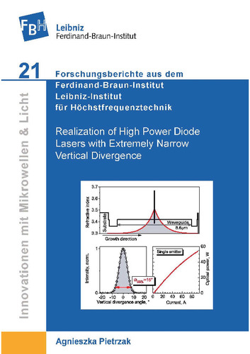
Through systematic model-based experimental investigations of a series of laser diode structures, the vertical beam divergence was reduced from 19° to 8.6° at full width at half maximum (FWHM) and from 30° to 15°, at 95% power content. The achieved vertical farfield angle is smaller, by a factor of ~3, than state-of-the-art laser devices. The 8 mm long and 200 μm wide single emitters based on the investigated SLOC structures deliver more than 30 W peak-power in quasi-continuous wave mode. The large equivalent spot-size together with the facet passivation prevent COMD failure and the maximum measured power is limited due to the overheating of the device. Moreover, a 4 mm long and 200 μm wide single emitter tested under ‘zero-heat’ condition delivers 124 W power. The maximal measured power was limited by the current supply.
| ISBN-10 (Impresion) | 3954040662 |
| ISBN-13 (Impresion) | 9783954040667 |
| ISBN-13 (E-Book) | 9783736940666 |
| Formato | A5 |
| Idioma | Inglés |
| Numero de paginas | 144 |
| Laminacion de la cubierta | mate |
| Edicion | 1 Aufl. |
| Serie | Innovationen mit Mikrowellen und Licht. Forschungsberichte aus dem Ferdinand-Braun-Institut, Leibniz-Institut für Höchstfrequenztechnik |
| Volumen | 21 |
| Lugar de publicacion | Göttingen |
| Lugar de la disertacion | Berlin |
| Fecha de publicacion | 18.04.2012 |
| Clasificacion simple | Tesis doctoral |
| Area |
Física
|


