Cuvillier Verlag GmbH
| Fachbereiche | |
|---|---|
| Buchreihen (98) |
1404
|
| Nachhaltigkeit |
3
|
| Gesundheitswesen |
2
|
| Geisteswissenschaften |
2395
|
| Naturwissenschaften |
5424
|
| Mathematik | 229 |
| Informatik | 320 |
| Physik | 981 |
| Chemie | 1369 |
| Geowissenschaften | 131 |
| Humanmedizin | 245 |
| Zahn-, Mund- und Kieferheilkunde | 10 |
| Veterinärmedizin | 112 |
| Pharmazie | 147 |
| Biologie | 837 |
| Biochemie, Molekularbiologie, Gentechnologie | 121 |
| Biophysik | 25 |
| Ernährungs- und Haushaltswissenschaften | 45 |
| Land- und Agrarwissenschaften | 1005 |
| Forstwissenschaften | 201 |
| Gartenbauwissenschaft | 20 |
| Umweltforschung, Ökologie und Landespflege | 148 |
| Ingenieurwissenschaften |
1814
|
| Allgemein |
99
|
|
Leitlinien Unfallchirurgie
5. Auflage bestellen |
|
Erweiterte Suche
Molecular Beam Epitaxy Growth and Characerization of ZnO-based layers and Heterostructures
Abdelhamid Abdelrehim Mahmoud Elshaer (Autor)Vorschau
Inhaltsverzeichnis, Datei (29 KB)
Leseprobe, Datei (35 KB)
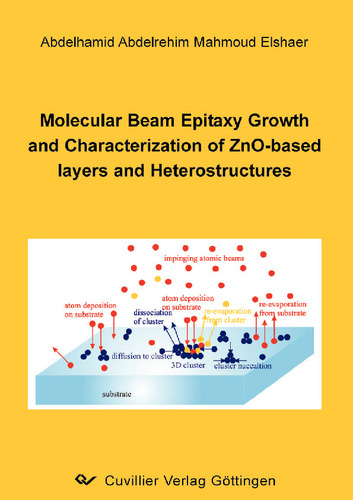
In semiconductor research a reliable epitaxial growth technique for growing high quality thin
films and heterostructures is necessary. In the case of ZnO one of the main difficulties is the
absence of suitable substrate material for ZnO epitaxial growth. Although special oxide
material (for example ScAlMgO4) and ZnO bulk crystal can serve as lattice matched
substrates, the quality of the substrates themselves, the size of the available wafer, and the
expense do not encourage to use these lattice matched substrates for ZnO epitaxial growth. In
the current research, a widely used low cost commercial substrate sapphire was employed to
develop a reliable epitaxial growth technique and growth process for ZnO. The versatile
epitaxial growth technique, molecular beam epitaxy (MBE) equipped with a rf-plasma source
was developed for growth and various characterizations methods were conducted to obtain a
fundamental understanding in both the epitaxial processes and material properties of ZnO thin
films and heterostructures.
Employing a thin HT MgO buffer layer prior to ZnO growth is the key to overcome the very
large mismatches between c-Al2O3 substrate. Wetting the surface of Al2O3 substrate with a
few MgO monolayers, lowed the surface energy, so that the lateral growth of ZnO is
promoted at the initial growth stage. MgO can be grown in the same chamber as ZnO without
any contamination problem. These advantages make the growth procedure of a HT MgO
buffer fast and easy. The growth temperature and the growth rate of MgO buffer are found to
be important to improve the ZnO heteroepitaxy. An intermediate spinel layer in epitaxial
relation with the sapphire substrate as well as with the HT MgO buffer layer is formed in the
early stage of growth during the deposition of the MgO at 700°C. It was found that the
combination of these two layers is useful for the progressive reduction of the ZnO overgrown
with the sapphire substrate.Annealing experiments reveal that as soon as the spinel layer is
formed at about 700°C, it remains stable at least up to 1000°C, and even it is extended in
thickness.
By recording and analyzing RHEED intensity oscillations, the growth kinetics has been
investigated. Flat surface morphology and layer-by-layer growth has been achieved. The
stoichiometry has been deduced by analyzing the growth rate as a function of Zn and O fluxes
for various growth temperatures. It is found that the sticking coefficient of oxygen radicals is
less dependent on the substrate temperature than that of Zn. The stoichiometric condition
shifts to larger Zn flux at higher growth temperature. The kink rZnO values determine the
activated O-flux supplied by the RF plasma source at TS=500°C, 400W and a given O2-flow
rate. It equals 0.5±0.05 Ås-1 per sccm. Absolute αZn values versus TS, defined as
αZn=rZnO(T)/rZnO(max), where rZnO(max) is recalculated from the Zn flux measured by a
quartz monitor, using Zn/ZnO molar mass and density ratios.
Ex-situ characterization of the grown ZnO layers indicate that the surface morphology and
crystal quality of the ZnO films grown on sapphire by MBE using either oxygen plasma cell
or H2O2 as an oxidant can be extensively improved by using an HT MgO buffer.
ZnO layers reveal strong variation of surface morphology versus the O/Zn flux ratio. The
most flat surface morphology of ZnO is obtained when the ratio is within the 0.7-1 range. The
growth under O-rich conditions leads to formation of hexagonal pyramids and at higher O/Zn
ratios to a 3D growth with the top layer formed by perfectly c-oriented columnar structures of
50-100 nm in a diameter. It was also possible to recover the initial 3D growth mode to the 2D
one by employing the Zn-rich growth conditions at O/Zn=0.4-0.6.
Structural characterizations by high resolution X-ray diffraction (HR-XRD) and transmission
electron microscopy (TEM) indicate a dramatic reduction in defect density in the ZnO
epilayers grown with an HT MgO buffer. By using TEM, it was found that the dominant
extending defects are edge, screw and mixed-type dislocations along c-axis. The main defects
were threading dislocations. This is resulted from the well controlled layer-by-layer growth,
since only the edge-type dislocation is able to accommodate the lattice mismatch, while the
screw type dislocation forms much related to the initial nucleation environment.The
microstructure of ZnO epilayers has been studied by HR-XRD. The full width at half
maximum of the (0002) reflection, 0.007 degree, is much smaller than that of the (10-10)
reflection, 0.27 degree revealing the micro-twist dominates the mosaicity, while micro-tilt is
much less important.This pronounced difference of the rocking curve widths between the
(0002) and (1010) reflections strongly indicates that the density of pure edge threading
dislocations is greater than that of pure screw dislocations.
Optical characterizations reveal that exciton plays an important role in ZnO. At room
temperature free exciton recombinations dominate the photoluminescence. The ZnO epilayers
reveal well resolved low temperature PL excitonic spectra with a dominant bound exciton line (3.355 eV) possessing a ~2 meV half-width and a peak of free A exciton at 3.374
eV. The low-energy tail extending from the excitonic emission peaks due to the lattice
deformation is significantly reduced, which allows the observation of two electron satellites
and LO-phonons replicas of free and bound excitons. Variation of growth stoichiometry from
O-rich to Zn-rich results in the pronounced quench of the acceptor-bound part of the excitonic
band, as well as the strong intensity redistribution of donor-bound lines which seems to be
attributed to a change in the point defect density. Temperature dependence of PL spectra
between 6K and room temperature every 30 K under the same excitation conditions was
performed. Slowly decreases coming at 300K to about one third of the intensity at 6K. This
corresponds to the activation of non-radiative channels in the capturing and recombination
processes. This result was confirm by decay time measurements. PL mapping of 2 inch ZnO
epilayer shows high lateral homogeneity from PL intensity distribution and PL FWHM
distribution.
Hall-effect measurements and Electrochemical profiling (ECV) were used to characterize the
electrical properties of ZnO samples. Hall-effect measurements indicated n-type behavior
with carrier concentration of 2.0×1016 cm-3 and mobility of approximately 96 cm2/Vs. ECV
profile versus depth measured for the top 2.5 μm thick sample gives surface carrier
concentration is 2.0×1016 cm-3 increasing to a maximum value of 1.0×1018 cm-3 the
semiconductor/substrate interface.
P-n heterojuntions and mesa structures comprising MBE n-ZnO layers and CVD p-4H-SiC
laser were manufactured and investigated. Electrical properties of the mesa diodes have been
studied with Hall measurements, and current-voltage measurements (I-V). I-V measurements
of the device show good rectifying behavior, from which a turn-on voltage of about 2 V was
obtained.
With the excitation of O and N gas mixture in a single plasma cell, followed by the sample
annealing procedure. P-type ZnO:N layers with a net hole concentration 3×1017 cm-3 using
was measured. The combination of low growth temperature, slightly O-rich conditions and
post-growth annealing is shown to be effective way to obtain p-doping. Further efforts are
necessary to improve structural quality of the low-temperature p-type ZnO:N films.
Optical properties of ZnO based II-VI heterostructures and quantum structures have also been
studied. The surface roughness of ZnxMg1−xO was as low as 0.7 nm. The optical band gap
and photoluminescence peak can be turned to larger energy with the same high crystallinity
and without significant change in the lattice constant. The prominent PL peaks related to the
SQW show a systematic blueshift with decreasing well width, which is consistent with the
quantum size effect. The SQW-related emission peaks exhibit an S-shaped (redshift-blueshiftredshift)
behaviour with increasing temperature, which is in contrast with that ascribed to
band gap shrinkage (redshift). The observed behavior is discussed in terms of localization at
lateral interface potential fluctuations. For T >70 K the integrated PL intensity is thermally
activated with activation energies much less than the band offsets. It is argued that the
dominant mechanism leading to the quenching of the ZnO SQW-related PL is due to the
thermionic emission of excitons out of the lateral potential minima caused by potential
fluctuations, such as interface fluctuations by 1 ML. Stimulated emission has been achieved at
room temperature in a separate confinement double heterostructure having a 3 nm wide SQW
as an active region. It has been found that a critical parameter for the lasing is the
inhomogeneous broadening of both QW and barrier emission bands.
MBE process for ZnO has been developed where high quality ZnO epilayers and
heterostructures can be grown by molecular beam epitaxy on sapphire substrate. For nitrogen
doping of ZnO, Oxygen and nitrogen were activated in the single plasma cell. No
reproducible and reliable experimental results on the achievement of p-type conductivity
achieved. Stimulated emission has been achieved at room temperature.
| ISBN-13 (Printausgabe) | 386727701X |
| ISBN-13 (Printausgabe) | 9783867277013 |
| ISBN-13 (E-Book) | 9783736927018 |
| Sprache | Englisch |
| Seitenanzahl | 144 |
| Auflage | 1 Aufl. |
| Band | 0 |
| Erscheinungsort | Göttingen |
| Promotionsort | Braunschweig |
| Erscheinungsdatum | 21.08.2008 |
| Allgemeine Einordnung | Dissertation |
| Fachbereiche |
Informatik
Physik Elektrotechnik |


