| Fachbereiche | |
|---|---|
| Buchreihen (97) |
1384
|
| Nachhaltigkeit |
3
|
| Gesundheitswesen |
1
|
| Geisteswissenschaften |
2380
|
| Naturwissenschaften |
5411
|
| Ingenieurwissenschaften |
1802
|
| Allgemeine Ingenieurwissenschaften | 292 |
| Maschinenbau und Verfahrenstechnik | 865 |
| Elektrotechnik | 691 |
| Bergbau- und Hüttenwesen | 30 |
| Architektur und Bauwesen | 76 |
| Allgemein |
98
|
|
Leitlinien Unfallchirurgie
5. Auflage bestellen |
|
Erweiterte Suche
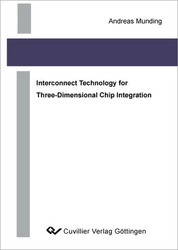
Interconnect Technology for Three-Dimensional Chip Integration
Andreas Munding (Autor)Vorschau
Inhaltsverzeichnis, Datei (35 KB)
Leseprobe, Datei (390 KB)
3D-integration, or vertical chip integration, is a technology that aims to shorten the interconnect path between integrated circuits and to increase the interconnect density by using through-chip micro vias. It allows a smaller ciruit footprint by chip-stacking and can combine a variety of technologies. This thesis treats the technologigal aspects of a novel 3D-integration concept, which is based on processes that follow the sequence: wafer thinning, via processing, chip stacking. The micro vias are processed from the backside and therefore do not impose routing restrictions on the front side of the circuit. As an example application, the two key elements, the micro vias and the micro joints are formed on bare silicon substrate. It is shown how an electrical interconnect path from the top to the bottom of a mechanically sound chip stack can be realized. The process of stacking employs a solder based bonding method, which results in a rigid and thermally stable connection. By solid-liquid interdiffusion (isothermal solidification) the solder filled connection zone is entirely transformed into intermetallic compounds. This results in a homogenized and rigid joint with excellent mechanical properties, suitable for step by step stack building. Further, the scaling of microjoints in such 3-dimensional chip-stacks is proposed by means of kinetic control. Therefore, phase growth in the copper-tin system in the presence of various metal barriers at the interface is evaluated. Promising results have been obtained by using layers of Ti, Ta, Ti:W or combilayers thereof in a thickness range of 20 to 50 nm. These results suggest a miniaturization potential of solder based microjoints down to the scale of 1 µm, along with the respective increase in interconnect density.
| ISBN-13 (Printausgabe) | 3867274061 |
| ISBN-13 (Printausgabe) | 9783867274067 |
| ISBN-13 (E-Book) | 9783736924062 |
| Buchendformat | A5 |
| Sprache | Englisch |
| Seitenanzahl | 138 |
| Auflage | 1 |
| Band | 0 |
| Erscheinungsort | Göttingen |
| Promotionsort | Ulm |
| Erscheinungsdatum | 30.10.2007 |
| Allgemeine Einordnung | Dissertation |
| Fachbereiche |
Elektrotechnik
|
| Schlagwörter | Mikrostrukturierung; Halbleitertechnologie. |


