| Areas | |
|---|---|
| Serie de libros (97) |
1384
|
| Nachhaltigkeit |
3
|
| Gesundheitswesen |
1
|
| Letra |
2380
|
| Ciencias Naturales |
5411
|
| Matemática | 228 |
| Informática | 320 |
| Física | 981 |
| Química | 1366 |
| Geociencias | 131 |
| Medicina humana | 243 |
| Estomatología | 10 |
| Veterinaria | 108 |
| Farmacia | 147 |
| Biología | 835 |
| Bioquímica, biología molecular, tecnología genética | 121 |
| Biofísica | 25 |
| Nutrición | 45 |
| Agricultura | 1005 |
| Silvicultura | 201 |
| Horticultura | 20 |
| Ecología y conservación de la tierra | 148 |
| Ciencias Ingeniería |
1802
|
| General |
98
|
|
Leitlinien Unfallchirurgie
5. Auflage bestellen |
|
Erweiterte Suche
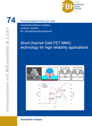
Short channel GaN FET MMIC technology for high reliability applications (Volumen 74) (Tienda española)
Günther Tränkle (Editor)Konstantin Osipov (Autor)
Previo
Lectura de prueba, PDF (380 KB)
Indice, PDF (160 KB)
Nowdays GaN HEMT technology reached maturity level that allows industral fabrication of such devices for wide range of civil (telecommunications, power electrinics, automotive etc.), as well as space and military (phased array radars) applications. At this level, technology start reaching physical limits of GaN material and require new approaches that will allow to overcome some of well known problems related to GaN HEMTs, such as high gate leakage currents, reliability issues and difficulties of normally-off transistor fabrication.
The goal of these theses is theoretical and experimental confirmation of the idea, that using peizoelectric nature of GaN crystal will allow local modification of GaN HEMT channel by means of external mechanical stress (using first and second passivation layers as stressors).
After implementation of the proposed technology changes and new device geometry in process flow intended for 150 nm GaN HEMT MMIC fabrication, E/D devices with pinch-off voltages +0.1V and -1.65V respectively were fabricated on the same wafer within single process flow. It was observed, that E-mode devices, fabricated using compressed passivation layers, demonstrate lower gate leakage currents and more robust in HTRB test as compared to D-mode devices.
In summary, it was demonstrated, that it is possible to control pinch-off voltage and gate leakage current of short channel GaN HEMTs by application of external stress. Usage of external stress, opens new degree of freedom in device optimization, and extends opportunities for more advanced MMIC design.
| ISBN-13 (Impresion) | 9783736979567 |
| ISBN-13 (E-Book) | 9783736969568 |
| Formato | A5 |
| Idioma | Inglés |
| Numero de paginas | 186 |
| Laminacion de la cubierta | mate |
| Edicion | 1. |
| Serie | Innovationen mit Mikrowellen und Licht. Forschungsberichte aus dem Ferdinand-Braun-Institut, Leibniz-Institut für Höchstfrequenztechnik |
| Volumen | 74 |
| Lugar de publicacion | Göttingen |
| Lugar de la disertacion | Berlin |
| Fecha de publicacion | 07.02.2024 |
| Clasificacion simple | Tesis doctoral |
| Area |
Informática
Ingeniería eléctrica |
| Palabras claves | Gate, process, GaN HEMT, SiNx, Passivation, Mechanical stress, Normally-off transistors, GaN MMiCs, Ir gate, transistors, performance, technology, transistor, metal, structure, resist, power, electron, device, power, effect, epitaxial, voltage, development, temperature, electrical, experiment, internal, devices, surface, passivation, external, structures, performed, mmic, concentration, semiconductor, maximum, influence, parameters, properties, compressive, fabricated, piezoelect, mechanical, ohmic |


