| Departments | |
|---|---|
| Book Series (98) |
1394
|
| Nachhaltigkeit |
3
|
| Gesundheitswesen |
1
|
| Humanities |
2383
|
| Natural Sciences |
5414
|
| Mathematics | 228 |
| Informatics | 320 |
| Physics | 981 |
| Chemistry | 1368 |
| Geosciences | 131 |
| Human medicine | 243 |
| Stomatology | 10 |
| Veterinary medicine | 109 |
| Pharmacy | 147 |
| Biology | 835 |
| Biochemistry, molecular biology, gene technology | 121 |
| Biophysics | 25 |
| Domestic and nutritional science | 45 |
| Agricultural science | 1005 |
| Forest science | 201 |
| Horticultural science | 20 |
| Environmental research, ecology and landscape conservation | 148 |
| Engineering |
1811
|
| Common |
98
|
|
Leitlinien Unfallchirurgie
5. Auflage bestellen |
|
Advanced Search
Nanoscale Electrodeposition of Ultrathin Magnetic Ni Films and of the Compound Semiconductors AlSb and ZnSb from Ionic Liquids (English shop)
Olivier Mann (Author)Preview
Table of Contents, Datei (51 KB)
Extract, Datei (160 KB)
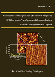
This thesis focuses on the 2D and 3D electrochemical phase formation of the metals Ni and Sb as well as the electrodeposition of the compound semiconductors AlSb and ZnSb at the electrified ionic liquid/Au(111) interface. These investigations were performed at the nanometer and partly the atomic scale. For this aim, the in situ electrochemical scanning probe microscopy (SPM) technique combined with conventional electrochemical methods such as cyclic voltammetry and chronoamperomerty were employed. In order to investigate the purity of the deposited films X-ray photoelectron spectroscopy method (XPS) has also been used. The electrodeposition of the compound semiconductors AlSb and ZnSb required the use of ionic liquids, AlCl3-[C4mim]Cl− and ZnCl2-[C4mim]Cl−, respectively, since these latter possess sufficiently large electrochemical windows. The main results of this thesis can be summarized as follows: A pronounced adsorption of anions on Au(111) for both ionic liquid is observed at anodic potentials above the underdeposition potential (UPD) of the metals; the structure of the respective adsorption films could be clarified for the first time. Thus, an incommensurate c(p×2√3) structure was found for adsorbed AlCl4− whereas the ZnCl3− layer exhibits the characteristics of a Moirée-like pattern.
In the overpotential region (OPD) of the 3D deposition of Ni (-0.25 V vs Ni/Ni2+) in an AlCl3-[C4mim]Cl− melt, a new morphology of Ni clusters could be obtained which formation follows an instantaneous nucleation and growth process. For this a complete monolayer of Ni was first deposited on Au(111) followed by a direct jump of the potential to -0.25 V. Thereby result Ni Clusters of cylindrical shape presenting a diameter of ~ 10 nm and an aspect ratio of ~ 2 in a 5 mM Ni2 solution. They are characterised by a dense packing and an orientation in one direction which is indicative of a magnetic interaction between the Ni clusters in concordance with the aspect ratio value. These results are therefore of application interest.
A typical (√3 × √3)R30° structure of the first monolayer is observed for the Sb UPD deposition in both ionic liquids. A second antimony layer can be formed under UPD conditions. In the OPD region different morphologies of the Sb deposits can be obtained depending on the deposition procedure. When the potential is continuously stepped to 0.1 V vs Al/Al3+ Sb nanostripes are formed whereas randomly dispersed small clusters of spherical shape are found if the potential is jumped from 0.0 V to -0.3 V vs Al/Al(III). These observations are consistent with appropriate investigations in the literature in which aqueous electrolytes were used. and p-doping of the clusters through the variation of the deposition potential in the vicinity of the stoichiometric semiconductor compound potential are reported.
For the first time the deposition of compound semiconductors on the nanometer scale was successfully performed by using ionic liquids as electrolytes. A Zn-based and an Al-based ionic liquid were used for the formation of ZnSb (-0.9 V vs Pt/Pt(II) quasi-reference) and AlSb (-1.1 V vs Al/Al3+), respectively. In both cases spherical clusters presenting a diameter of ~ 10-20 nm were obtained whose electronic structures were clarified in situ by means of scanning tunneling spectroscopy (STS). With this size of clusters the band gaps of 2.0 ± 0.2 eV (AlSb) and 0.6 ± 0.1 eV (ZnSb) of the respective bulk phases could be reproduced. First experiments of the respective n
| ISBN-13 (Printausgabe) | 3867275041 |
| ISBN-13 (Hard Copy) | 9783867275040 |
| ISBN-13 (eBook) | 9783736925045 |
| Final Book Format | A5 |
| Language | English |
| Page Number | 152 |
| Edition | 1 |
| Volume | 0 |
| Publication Place | Göttingen |
| Place of Dissertation | Karlsruhe |
| Publication Date | 2008-01-29 |
| General Categorization | Dissertation |
| Departments |
Chemistry
|


