
Cuvillier Verlag GmbH



| Departments | |
|---|---|
| Book Series (99) |
1415
|
| Nachhaltigkeit |
3
|
| Gesundheitswesen |
3
|
| Humanities |
2412
|
| Natural Sciences |
5430
|
| Engineering |
1821
|
| Engineering | 292 |
| Mechanical and process engineering | 872 |
| Electrical engineering | 700 |
| Mining and metallurgy | 30 |
| Architecture and civil engineering | 76 |
| Common |
97
|
|
Leitlinien Unfallchirurgie
5. Auflage bestellen |
|
Advanced Search
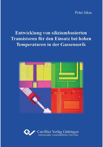
Entwicklung von siliziumbasierten Transistoren für den Einsatz bei hohen Temperaturen in der Gassensorik (English shop)
Peter Iskra (Author)Preview
Table of Contents, Datei (53 KB)
Extract, Datei (200 KB)
This work compares different MOSFET concepts with regard to their temperature stability. Furthermore, one of the concepts is integrated into a field-effect gas sensor and characterised. The MOSFET concepts comprise, on the one hand, lateral and, on the other hand, vertical transistors. The lateral MOSFET variant is built on silicon and SOI (Silicon On Insulator) substrates. Through the use of SOI substrates, a significant increase in temperature stability can be achieved. Owing to the process sequence, the vertical MOSFET variant offers a simple means of realising short channel lengths and high channel doping levels. Especially because of the high channel doping, this concept is predestined for the construction of temperature-stable MOSFETs. Further temperature ruggedness of the vertical MOSFETs can be gained by modifying the channel doping profile. A vertical read-out transistor is employed in the fabricated gas sensor. The function of the sensor is demonstrated by means of gas measurements. At the beginning of the work, the change in device behaviour as a result of increasing temperature is discussed. A particularly critical temperature effect is the increasing OFF current. The cause of this increase lies in rising leakage currents at the reverse-biased pn junctions. Their suppression can be achieved both by reducing the pn junction area and by high doping levels. A high dopant concentration ensures the extrinsic state of the semiconductor, and thus the blocking function of the pn junction, even at elevated temperatures. The approach of increasing temperature stability by reducing the pn junction area is implemented in lateral transistors by building them on SOI substrates. For this purpose, the MOSFETs are placed on a thin silicon layer. The doped regions thereby predominantly adjoin an oxide layer that is isolated from the substrate. The channel region of the SOI MOSFETs is not electrically contacted, which can give rise to additional effects. The most important of these is the kink effect, in which the channel region becomes charged and leads to a drain current that no longer saturates in the output characteristics. The enhancement of temperature ruggedness by increasing the dopant concentration comes into play in vertical MOSFETs. However, limits exist in the choice of the dopant concentration. Excessively high doping leads, owing to a band-to-band tunnelling process, to breakdown of the pn junction already at room temperature. Consequently, a compromise must be found between temperature ruggedness and tunnelling breakdown. Furthermore, to suppress tunnelling breakdown, there is the possibility of embedding an intrinsic layer between the p- and n-doped zones. A vertical n-channel transistor is then formed by a nipin layer stack. The intrinsic layer increases the tunnelling width and permits higher doping levels for the p- and n-regions. The gas sensor fabricated in this work represents a further development of an already commercially available variant. Because of the technology used, this standard variant can only be operated up to a temperature of 200 °C. For numerous applications, however, a higher temperature stability is desired. Therefore, a gas sensor optimised with respect to temperature ruggedness is fabricated in this work. Essential differences from the standard variant lie in a vertical MOSFET concept as well as a construction on SOI substrates. The fabrication of the different devices requires the development and optimisation of numerous process technologies. Thus, in the vertical MOSFET concept, the focus lies on the vapour phase deposition of the transistor layer stack, the dry chemical patterning of the mesa, and the growth or deposition of the gate dielectric. In the vapour phase deposition, the processes for realising an npn and a nipin layer stack are first developed. Furthermore, different concepts for building vertical pnp MOSFETs are also presented. An important prerequisite for the deposition of high-quality layers is an effective pre-cleaning of the substrates. To this end, three different cleaning procedures are compared. A dry chemical etching process serves for the subsequent patterning of the layer stack. This is optimised with regard to the necessary smooth and steep etch sidewalls. For this purpose, numerous parameters of the etching process as well as of the preceding lithography are varied and their influence on the patterning is assessed. The result is an optimised etching process. The temperature stability of the devices requires the sharpest possible doping profile. Therefore, the thermal budget of the subsequent fabrication of the gate dielectric must be kept as low as possible. The approaches investigated for this are, on the one hand, thermal low-temperature oxides and, on the other hand, two-layer systems consisting of a thermal oxide and a deposited silicon nitride. Both gate dielectrics are employed in device fabrication. The construction of the lateral transistor also requires development work in some process steps. The focus here is on the doping of the source and drain regions by means of Spin On Dopants (SOD). Process optimisation is carried out for the layer deposition as well as the subsequent dopant drive-in. The electrical characterisation of the devices is carried out both at room temperature and at elevated temperatures. The transfer and output characteristics of the MOSFETs are recorded. From the characteristics, the device parameters are derived and compared with one another. Both lateral MOSFET variants show the characteristic device behaviour of a long-channel transistor. The determined subthreshold slope corresponds to the theoretical minimum of 60 mV/dec. Owing to the smaller pn junction area, the MOSFET on the SOI substrate exhibits an OFF current that is two decades lower. This difference is maintained up to the maximum investigated temperature of 200 °C. At this temperature, the ION/IOFF ratio falls to 4.2 decades for the SOI MOSFET and to only 2.2 decades for the Si MOSFET. With a channel length of 220 nm, the fabricated vertical npn MOSFET belongs to the short-channel transistors. Consequently, the typical effects such as channel length modulation occur in this device. Furthermore, the channel region is not electrically contacted, which manifests itself in the floating body effects already known from SOI MOSFETs. The high channel doping necessary for temperature stability causes an increase in the subthreshold slope to 158 mV/dec. At the same time, owing to the band-to-band tunnelling current, the OFF current lies about 4 decades above that of the lateral SOI MOSFET. The advantage of the vertical transistor becomes apparent in the ION/IOFF ratio at 200 °C. This amounts to 5.2 decades and thus lies a further decade above that of the SOI MOSFET. Further measurements show the full functionality of the MOSFET at 400 °C with an ION/IOFF ratio of one decade. A further option for increasing temperature ruggedness is offered by the construction of a nipin MOSFET. Its additional intrinsic zones suppress the band-to-band tunnelling current, whereby an additional increase in the dopant concentration becomes possible for the channel region. The nipin MOSFET fabricated in this work exhibits an OFF current that is 4 decades lower compared with the vertical npn MOSFET. However, the incorporation of the intrinsic zones also brings about a change in the device behaviour. As a result of an impact ionisation process in the intrinsic region, a very rapid turn-on of the MOSFET is observed above a sufficiently high gate voltage. This so-called ionisation mode is based on the aforementioned kink effect. The subthreshold slope of the investigated MOSFET amounts to 27 mV/dec in the ionisation mode. With increasing temperature, the impact ionisation collapses and the switching dynamics decrease strongly. Although the channel doping of the fabricated nipin MOSFET was increased, the ION/IOFF ratio at 200 °C, at 4.9 decades, lies approximately at the level of the npn MOSFET. The cause of this lies in the diffusion and the associated drop in the maximum channel doping during the fabrication of the gate oxide. Despite the introduction of a two-layer gate dielectric, the temperature budget could not be reduced sufficiently. For further work, metal-organic vapour phase epitaxy of the dielectrics is recommended. Furthermore, a dependence of the device parameters of the investigated nipin MOSFETs on the orientation on the substrate can be demonstrated. The difference is attributed to the growth rate of the gate oxide, which depends on the crystal plane. Finally, the gas sensor fabricated in this work is also characterised. At the operating point, it shows a strongly drifting baseline signal. The cause of the instability lies in a Fowler-Nordheim tunnelling current through the thin gate oxide. Only through conditioning prior to the gas measurement can the sensor be operated in a quasi-stable state at room temperature. The measurement signal then unambiguously reflects the gas exposure.
| ISBN-13 (Printausgabe) | 3954040328 |
| ISBN-13 (Hard Copy) | 9783954040322 |
| ISBN-13 (eBook) | 9783736940321 |
| Final Book Format | A5 |
| Language | German |
| Page Number | 240 |
| Lamination of Cover | glossy |
| Edition | 1 Aufl. |
| Volume | 0 |
| Publication Place | Göttingen |
| Place of Dissertation | München |
| Publication Date | 2012-02-28 |
| General Categorization | Dissertation |
| Departments |
Electrical engineering
|


