
Cuvillier Verlag GmbH



| Departments | |
|---|---|
| Book Series (99) |
1415
|
| Nachhaltigkeit |
3
|
| Gesundheitswesen |
3
|
| Humanities |
2412
|
| Natural Sciences |
5430
|
| Engineering |
1821
|
| Engineering | 292 |
| Mechanical and process engineering | 872 |
| Electrical engineering | 700 |
| Mining and metallurgy | 30 |
| Architecture and civil engineering | 76 |
| Common |
97
|
|
Leitlinien Unfallchirurgie
5. Auflage bestellen |
|
Advanced Search
Quantenmechanische und ballistische Nanobauelemente auf Siliziumbasis (English shop)
Lothar Höllt (Author)Preview
Table of Contents, Datei (48 KB)
Extract, Datei (110 KB)
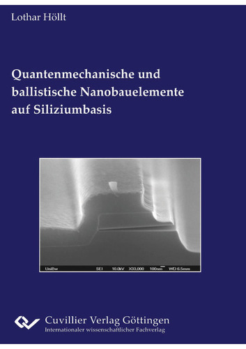
The subject of this thesis is the technology development and process integration for fabricating a prototype of the VFD SONFET and comparing its electrical characterization with simulations.
In this work, the world’s first VFD SONFET with a channel length in the range of 20 nm was electrically characterized. The measurement results demonstrate the feasibility of fabricating a VFD SONFET and show MOSFET-typical characteristics.
The focus of the technological development was on developing a SiGe sacrificial technique with a high selectivity between silicon and SiGe. The aim is to remove the approximately 2 µm wide SiGe sacrificial layer without destroying either the channel region, which is only about 30 nm thick, or the source layer. To this end, the complex interplay between the properties of the SiGe sacrificial layer, the source and channel layers, and the etching solution was first investigated.
To enable single-crystalline growth of the source layer, the SiGe sacrificial layer must be pseudomorphically strained. At the same time, the germanium content must be maximized in order to ensure a high selectivity for the etching process. To achieve this, a three-layer SiGe sacrificial layer with a highly doped germanium layer in the middle was developed. This maximizes the germanium content and thus the selectivity, while still ensuring a pseudomorphically strained crystal structure. For the VFD SONFET, a selectivity of 90 was achieved for the developed SiGe layer stack and an n-substrate.
This selectivity is lower than for exposed SiGe layers, since mass transport in the etched-out gap affects the reaction rate. The use of an ultrasonic bath does increase the selectivity, but the mechanical stress also destroys the free-standing source layer.
The electrical behavior of the VFD SONFET was characterized and simulated using simple models. The results of these simulations underline the advantage of the SON over the SOI structure and provide valuable information on the optimal parameters of the VFD SONFET.
| ISBN-13 (Printausgabe) | 3867279691 |
| ISBN-13 (Hard Copy) | 9783867279697 |
| ISBN-13 (eBook) | 9783736929692 |
| Language | German |
| Page Number | 186 |
| Edition | 1 Aufl. |
| Volume | 0 |
| Publication Place | Göttingen |
| Place of Dissertation | Universität der Bundeswehr München |
| Publication Date | 2009-05-29 |
| General Categorization | Dissertation |
| Departments |
Electrical engineering
|


