
Cuvillier Verlag GmbH



| Departments | |
|---|---|
| Book Series (99) |
1415
|
| Nachhaltigkeit |
3
|
| Gesundheitswesen |
3
|
| Humanities |
2410
|
| Natural Sciences |
5428
|
| Mathematics | 229 |
| Informatics | 320 |
| Physics | 982 |
| Chemistry | 1371 |
| Geosciences | 131 |
| Human medicine | 246 |
| Stomatology | 10 |
| Veterinary medicine | 112 |
| Pharmacy | 147 |
| Biology | 837 |
| Biochemistry, molecular biology, gene technology | 121 |
| Biophysics | 25 |
| Domestic and nutritional science | 45 |
| Agricultural science | 1005 |
| Forest science | 201 |
| Horticultural science | 20 |
| Environmental research, ecology and landscape conservation | 148 |
| Engineering |
1821
|
| Common |
97
|
|
Leitlinien Unfallchirurgie
5. Auflage bestellen |
|
Advanced Search
Herstellung freistehender Galliumnitrid-Schichten (English shop)
Peter Brückner (Author)Preview
Table of Contents, Datei (61 KB)
Extract, Datei (220 KB)
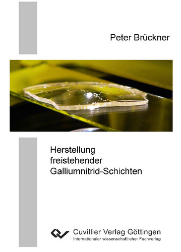
This work addresses the fabrication of free-standing gallium nitride layers by means of hydride vapour phase epitaxy (HVPE). The availability of low-defect GaN layers is important for improving the quality, efficiency and yield in the fabrication of modern electronic and optoelectronic devices based on GaN. Modern methods for producing low-defect layers on foreign substrates are reaching their limits, which are set by the large mismatch between the foreign substrate and GaN. One way out is growth on GaN substrates (homoepitaxy). This work therefore investigates possible routes and processes for producing free-standing GaN substrates.
The HVPE growth parameters and system properties for producing free-standing GaN substrates were carefully optimised. For thick layers it is necessary to achieve a high growth rate together with good material quality. The decisive factor here is the ratio between hydrogen and nitrogen, which should be around 50% in order to enable crack-free growth in the given configuration of the HVPE system. In particular, through a suitable choice of the growth parameters at the end of the growth process and slightly misoriented seed layers, the rough surface structure of HVPE layers could be improved. The surfaces optimised in this way are comparable to smooth MOVPE layers and require no further surface polishing in order to be used as quasi-substrates for a subsequent epitaxial process. Through the optimisation of the process parameters it was possible to realise layer thicknesses of more than 1.4 mm in a single growth experiment on a 2-inch wafer.
The methods for fabricating free-standing GaN samples investigated and discussed in this work can be broadly divided into two groups. On the one hand there are processes that require ex-situ steps, and on the other hand processes that can be realised entirely within a single system. Ex-situ processes are the laser-assisted lift-off of GaN layers, as well as growth on silicon, which can easily be removed in a wet-chemical etching solution. A further way of realising free-standing samples with an ex-situ process, in which the separation, however, occurs in-situ during cooling, is growth on lithographically structured dielectric masks (ELO). The samples produced in this way, although only 5×8 mm in size and 600 μm thick, showed excellent material properties. A carrier mobility of 810 cm²/Vs with a carrier density of 1.2×10^16 cm^-3 at room temperature and a defect density of 3×10^6 cm^-2 could be demonstrated. The most elegant way of producing free-standing GaN layers is to realise the separation layer for self-separation together with the thick GaN layer in a single growth run. For this purpose a low-temperature interlayer was deposited, which leads to the lift-off of the thick GaN layer. SiN layers can likewise serve as a separation layer. On these, the spontaneous separation of GaN layers up to 1.2 mm thick with a size of almost 2 inches could be observed.
| ISBN-13 (Printausgabe) | 3867278687 |
| ISBN-13 (Hard Copy) | 9783867278683 |
| ISBN-13 (eBook) | 9783736928688 |
| Language | German |
| Page Number | 154 |
| Edition | 1 Aufl. |
| Volume | 0 |
| Publication Place | Göttingen |
| Place of Dissertation | Universität Ulm |
| Publication Date | 2009-01-29 |
| General Categorization | Dissertation |
| Departments |
Physics
Engineering |
| Keywords | GaN, gallium nitride, substrate, free-standing, HVPE, hydride vapour phase epitaxy, bulk material, bulk, in situ, SiN, silicon nitride |


