
Cuvillier Verlag GmbH



| Departments | |
|---|---|
| Book Series (99) |
1415
|
| Nachhaltigkeit |
3
|
| Gesundheitswesen |
3
|
| Humanities |
2413
|
| Natural Sciences |
5430
|
| Mathematics | 230 |
| Informatics | 320 |
| Physics | 982 |
| Chemistry | 1371 |
| Geosciences | 131 |
| Human medicine | 246 |
| Stomatology | 10 |
| Veterinary medicine | 112 |
| Pharmacy | 147 |
| Biology | 837 |
| Biochemistry, molecular biology, gene technology | 121 |
| Biophysics | 25 |
| Domestic and nutritional science | 45 |
| Agricultural science | 1006 |
| Forest science | 201 |
| Horticultural science | 20 |
| Environmental research, ecology and landscape conservation | 149 |
| Engineering |
1822
|
| Common |
97
|
|
Leitlinien Unfallchirurgie
5. Auflage bestellen |
|
Advanced Search
Wachstum von Nanodrähten mittels der Metallorganischen Gasphasenepitaxie (English shop)
Ingo Regolin (Author)Preview
Table of Contents, Datei (38 KB)
Extract, Datei (93 KB)
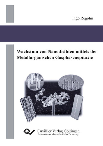
Within the framework of this dissertation, the growth of III/V nanowires by MOVPE was developed. In the course of work on various sub-areas, the basis was created for fabricating electronic and optoelectronic nanowire devices. On the way towards InAs field-effect transistors with very high mobilities and transconductance values, as well as nanowire-based GaAs light-emitting diodes, the growth of the nanowires had to be investigated and optimised with respect to structural properties, compositions, the creation of heterostructures and dopability. In this work, an essential contribution was made in particular in the field of p-doping of GaAs nanowires.
The VLS growth model, which served as the basis of this work, was discussed in detail. In addition, several methods were presented showing how and in what form the growth seeds can be deposited and also pre-patterned. In this work, gold nanoparticles were mainly used, which were deposited onto the sample surface prior to growth either from a colloidal solution or from the gas phase. Thin gold films were likewise used as growth templates, which are extremely interesting owing to their patternability during the evaporation process.
GaAs is the central material system with which most growth experiments were carried out. Here, detailed investigations regarding growth rate and structural form were performed in the course of this work. Crystal defects could be almost completely suppressed, as could superimposed shell growth, which is undesirable in some areas. The dependence of the growth rate on growth temperature, particle size and particle density was investigated over wide ranges with the aid of various SEM images. Moreover, it was possible to grow GaAs nanowires using iron particles, whereby the results demonstrate that these structures did not form via a VLS process.
Within the InxGa1-xAs material system, nanowires were realised in which the In content was varied in a controlled manner between 0 % and 100 %, thus covering the entire wavelength range between InAs and GaAs. For composition determination, high-resolution X-ray diffractometry could be successfully adapted for nanowires. The results were confirmed by means of high-resolution TEM characterisation including EDS analyses.
Heterostructures were realised in the framework of this work in both axial and radial arrangements, whereby for the shells the targeted transition from VLS to layer growth was exploited. The interface sharpness of axial GaAs/GaP/GaAs superstructures could be improved up to the resolution limit of the EDS measurement method used, with the aid of optimised growth interruptions during the group-V switching. GaAs/InxGa1-xAs/GaAs heterostructures could be produced in both the axial and the radial direction. Here, the axial material change, which is produced exclusively by the VLS mode, shows no abrupt transition, which can be attributed to the memory effect of the group-III elements within the gold particles. The radial transitions, which by contrast were formed by superposition with conventional layer growth, show sharp core-shell GaAs/InGaAs/GaAs transitions on the basis of EDS measurements. Furthermore, high-quality GaAs nanowires could be grown on Si substrate, which was demonstrated by intense photoluminescence. A preferred growth direction was only discernible after optimised surface preparation by means of HF etching steps as well as elevated annealing temperatures. The best results to date were achieved with externally prepared samples, on which short silicon nanowire stubs had already been pre-grown on a (111) silicon substrate by MBE.
In comparison to the structural properties of various semiconductor nanowires and nanowire heterostructures, there currently exist few results on controlled doping. However, the doping of semiconductor materials is the prerequisite for the fabrication of electronic and optoelectronic devices. Therefore, the doping of nanowires was an essential sub-area of this work. In order to address the doping problem of nanowires described above, different approaches were pursued. Using the p-dopant DEZn, GaAs nanowires could be successfully doped. At present it must be assumed that the Zn dopant reaches the wire via the gold particle. Since zinc can be dissolved in gold in arbitrary amounts and there is therefore no fixed saturation limit, a concentration gradient along the wire is observed which depends strongly on the Zn supply. Stationary carrier concentrations may well only be established after a wire length of several μm. By varying the zinc supply, carrier concentrations between 4.6×10 18
cm -3 and 2.3×10 19 cm -3 could be set. Si (n) or C (p) doping by means of the source materials DitBuSi and CBr4 is not feasible within VLS growth for the growth conditions chosen in this work. In the case of tapered structures, which form at higher growth temperatures, p-doped nanowire shells could be realised using CBr4. In addition to the in-situ MOVPE doping approaches, ion implantation was established as a successful alternative method for doping GaAs nanowires. By implanting Zn acceptors and a subsequent annealing procedure, the conductivity could be increased by a factor of 10 4
. Moreover, the amorphised structure reconstructs almost completely during this annealing step. Calculations on this show that a dopant concentration of about 3.5×10¹⁸
cm -3 could be achieved.
As the first nanowire devices, MISFETs were fabricated from InAs nanowires with excellent saturation behaviour and very high output currents. In addition, a very high transconductance value could be extracted, which can be attributed to the excellent material quality of the grown InAs structures. Although these structures are nominally undoped, n-type conductivity was demonstrated with the aid of these transistor data. This property could be explained by Fermi level pinning within the conduction band, which results in an electron accumulation at the surface. Moreover, a further contribution to this effect may also originate from a carbon background doping from the source materials. By combining p-doped GaAs nanowires grown on n-GaAs substrate, pn junctions could be fabricated which, in addition to the expected diode characteristics, show strong electroluminescence.
The present work ensured the scientific material supply for a number of projects of the department, such as the Collaborative Research Centre SFB 445. In addition, this dissertation contributed decisively to the development of the research focus on nanotechnology, for which highly topical new research tasks could be acquired. The future focus thus remains the doping and the associated realisation of pn junctions within a nanowire, in order to produce light-emitting diodes, solar cells and other devices.
| ISBN-13 (Printausgabe) | 3869555246 |
| ISBN-13 (Hard Copy) | 9783869555249 |
| ISBN-13 (eBook) | 9783736935242 |
| Language | German |
| Page Number | 148 |
| Edition | 1 Aufl. |
| Volume | 0 |
| Publication Place | Göttingen |
| Place of Dissertation | Duisburg |
| Publication Date | 2010-10-19 |
| General Categorization | Dissertation |
| Departments |
Physics
Electrical engineering |
| Keywords | Nanowires, VLS growth, doping, MOVPE, GaAs |


